


AlN具有极高的临界电场、高关态阻断电压、超低导通电阻、超快开关速度以及耐恶劣环境等优势,成为制备耐高压、高温电力电子器件的理想选择。AlN 器件的功率处理能力是SiC和GaN的15倍,因此被冠名为“下一代电力电子器件材料”,此外开发单晶低位错密度AlN衬底(小于103 cm-2)是实现高质量富Al成分AlGaN 薄膜的基础,在AlN同质衬底上生长富Al成分AlGaN 薄膜与蓝宝石衬底相比可使电阻率极大下降。国外已在大功率晶体管、半导体激光器、大规模集成电路、固体继电器和开关电源等大功率器件上得到成功应用。
大功率晶体管
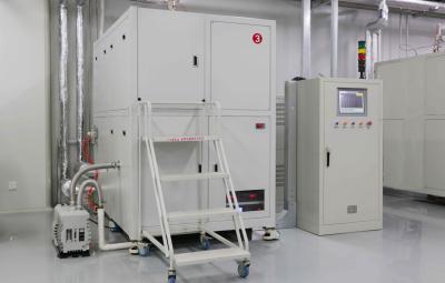
大功率绝缘栅双极晶体管(IGBT)是能源变换与传输的核心器件,俗称电力电子装置的“CPU”,作为国家战略性新兴产业,在轨道交通、智能电网、航空航天、电动汽车与新能源装备等领域应用极广。采用新型薄 AlN 衬底制作的大功率绝缘栅双极晶体管 ( IGBT) 模块,实现了高热耗散能力和高功率密度。新能源汽车的核心技术包含动力电池、电机和控制系统。而在控制系统中需要使用大量的 IGBT,如电机控制系统、车载空调控制系统、充电系统等。IGBT 在新能源汽车中发挥了重要的作用,是新能源汽车中的核心器件之一。
半导体激光器
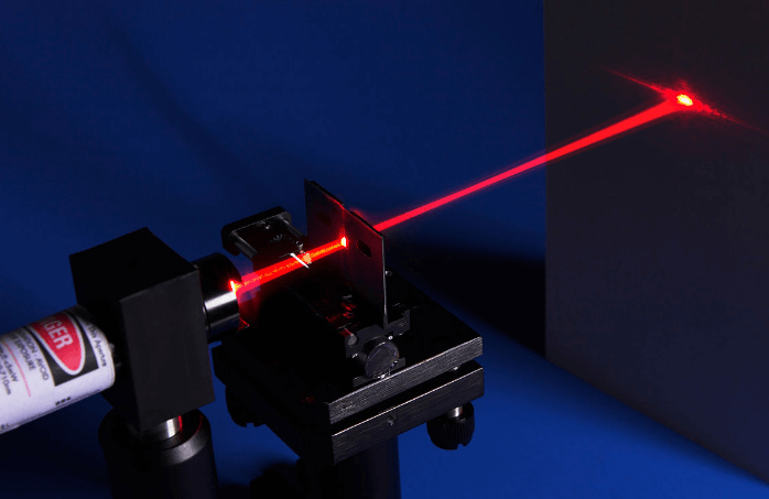
半导体激光器或激光二极管通过提供廉价且紧凑的激光器在我们的日常生活中发挥重要作用。 它们由要求纳米级精度和复杂设计的复杂多层结构组成。其工作原理是通过一定的激励方式,在半导体物质的能带(导带与价带)之间,或者半导体物质的能带与杂质(受主或施主)能级之间,实现非平衡载流子的粒子数反转,当处于粒子数反转状态的大量电子与空穴复合时,便产生受激发射作用。AlN超宽禁带,电子漂移饱和速度高,介电常数小等优势在制作大功率半导体激光器方面有不错应用前景。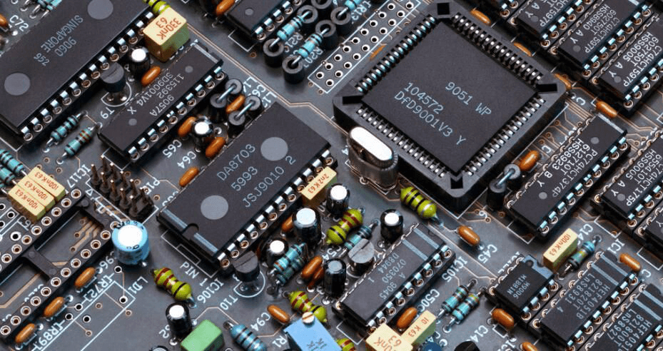
大规模集成电路
大规模集成电路指含逻辑门数为100门~9999门(或含元件数1000个~99999个),在一个芯片上集合有1000个以上电子元件的集成电路。采用一定的工艺,把一个电路中所需的晶体管、二极管、电阻、电容和电感等元件及布线互连一起,制作在一小块或几小块半导体晶片或介质基片上,然后封装在一个管壳内,成为具有所需电路功能的微型结构;其中所有元件在结构上已组成一个整体。AlN可应用于大规模集成电路的制作中,为信息产业发展提供有力支撑。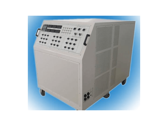
逆变器
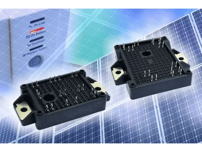
光伏逆变器的导热型 AlN 功率模块,这种采用 SiC 沟槽型 MOSFET 的半桥和全桥功率模块使用了AlN衬底混合式集成栅驱动器,采用电-热联合仿真和Al热沉,实现了高开关频率和低热阻,直接键合铜 AlN 衬底厚度为 0.63 mm,最大输出功率2 kW,功率密度为3.14 kW/l,超高热导率为170 W·m-1·K-1,为实现小型、高效电力电子系统提供了支撑。
功率开关
带有等离子体增强原子层淀积 (PEALD) AlN/GaN异质结构的新型垂直 GaN 沟槽结构功率器件,新结构在完成n-高阻层-n GaN外延沟槽刻蚀之后采用PEALD法淀积了3~5 nm厚的AlN层,实现了具有高电子密度和迁移率的垂直2DEG沟道,阈值电压为 2V,与传统GaN MOSFET相比,这种新型器件实现了9倍跨导和9 kA/cm2的极高漏电流密度,在未来功率开关领域具有应用优势。