


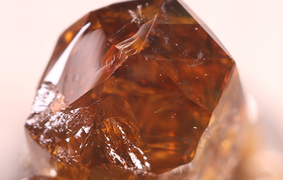

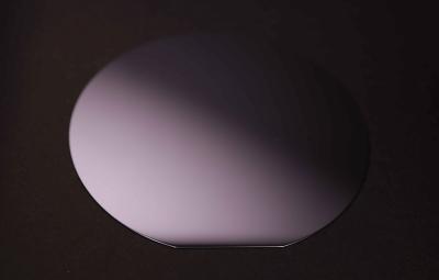


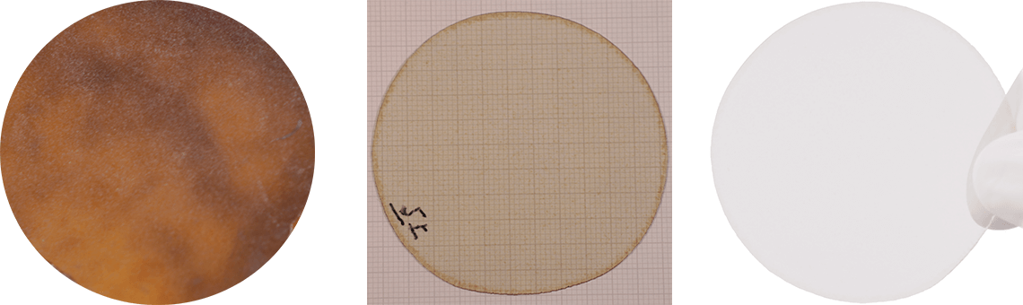
Successfully launched world-first Φ 60 mm AlN single crystals and single crystalline wafers.
Invited by the committee of the international conference on Light-Emitting Devices and Their Industrial Applications (LEDIA-2019), Ultratrend Technologies Co., Ltd. officially launched world-first Φ 60 mm AlN single crystalline wafers on April 24 at Pacifico Yokohama, Japan. LEDIA-2019 was held on 23-25 April and chaired by Nobel Laureate Prof. Hiroshi Amano. The launched wafers showed world-leading performance revealed by Raman spectroscopy and optical transmission spectra. The Raman spectroscopy exhibits an E2 (high) linewidth at half maximum of 2.85 cm-1,and the entire wafers exhibit excellent UV transparency with the absorption coefficient of 14-21 cm-1 in the UV range of 260-280 nm. The relevant results were published in the famous academic journal Physica Status Solidi A, and chosen as the cover of this journal as well. This achievement means that Ultratrend Technologies Co., Ltd. has made an important breakthrough on this key strategic ultra-wide bandgap semiconductor material. Before this milestone, the largest size of reported AlN single crystalline wafers is 50.8 mm, and suck kind of wafers can only be fabricated with very limited volume.
AlN is a typical kind of ultra-wide direct band-gap semiconductor material which has excellent properties, such as ultra-wide band-gap, high thermal conductivity, high resistivity, high chemical stability, high critical breakdown field strength, high carrier mobility, and high Ultraviolet transparency. As a consequence, AlN has become one of the most concerned new semiconductor materials and is also a key strategic new material that needs to be broken through. AlN wafer is the best candidate for high power, high-frequency electronic devices and optoelectronic devices such as ultraviolet detector, ultraviolet laser, and deep ultraviolet LED. They have wide application prospects in cutting-edge scientific and technological fields such as national defense, aerospace, secure communication/wireless communication, chip manufacturing, environmental protection and biomedical field. This important breakthrough by Ultratrend Technologies Co., Ltd. has laid a solid foundation for large-scale industrial applications worldwide.

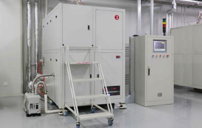
In the past 50 years, countries around the world have spent tremendous efforts to develop large-size AlN single crystals, but progress is very slow. Ultratrend Technologies Co., Ltd. is a hi-tech innovative enterprise established and led by renowned Chinese overseas professionals from the semiconductor industry. It focuses on the R&D of high-end PVT growth reactors, growth of ultra-wide band-gap semiconductor AlN single crystals, AlN wafers/templates, and related products. Over the past few years, Ultratrend Technologies Co., Ltd. has input a large number of R&D resources and capital, and successfully developed the world-first fully automatic 4-inch AlN crystal growth reactors with proprietary intellectual property rights, and a series of unique patented technologies for Φ 60 mm AlN single crystal growth and wafering processes. Nearly 30 international and domestic patents have been applied/granted. It has become one of the few hi-tech enterprises that have full AlN fabrication capabilities to produce large-size and high-quality AlN boules/wafers/templates worldwide.